7.3 Lvpwell
This drawn layer is defined for 3.3V and 5V/6V NMOS body . If this layer is used without DNWELL (outside DNWELL), the body of all those transistors will by default be connected to P-substrate potential. If LVPWELL is designed as a resistor, it is not allowed to be placed outside DNWELL.
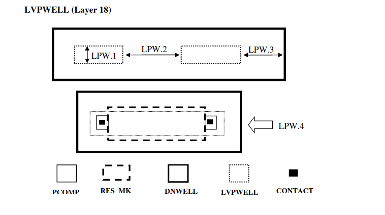
(A) LVPWELL Inside DNWELL
RULE NO. |
DESCRIPTION |
LAYOUT |
|
Layer |
LPW = LVPWELL |
3.3V |
5V/6V |
LPW.1 |
Min. LVPWELL Width |
0.6 |
0.74 |
LPW.2a |
Min. LVPWELL to LVPWELL Space (Inside DNWELL) [Different potential] |
1.4 |
1.7 |
LPW.2b |
Min. LVPWELL to LVPWELL Space [Equi potential] |
0.86 |
0.86 |
LPW.3 |
Min. DNWELL enclose LVPWELL |
2.5 |
2.5 |
LPW.4* |
If LVPWELL is used as resistor, it must be covered by RES_MK (for LVS purpose). Width of the resistor determined by LVPWELL. Length by COMP-to-COMP space. RES_MK length shall be coinciding with resistor length (Touching COMP each side) and width covering the width of LVPWELL. |
||
LPW.5 |
LVPWELL resistors must be enclosed by DNWELL |
||
Note.1 ** |
Recommended Min. width to achieve stable LVPWELL resistor. |
2 |
2 |
Note
** This note is a layout guide for customer and this rule can be detected by ERC, not by DRC
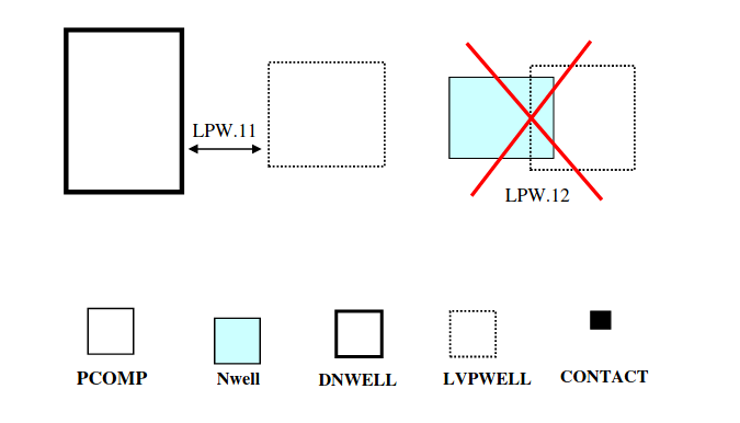
(B) LVPWELL Outside DNWELL
RULE NO. |
DESCRIPTION |
LAYOUT |
Layer |
LPW = LVPWELL |
|
LPW.11 |
Min (LVPWELL outside DNWELL) space to DNWELL |
1.5 |
LPW.12 |
LVPWELL cannot overlap with Nwell |