7.8 Nplus
RULE NO. |
DESCRIPTION |
LAYOUT RULE |
Layer |
NP = Nplus Implant |
|
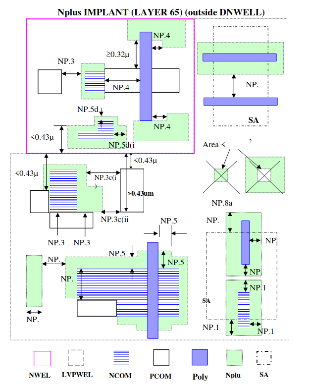
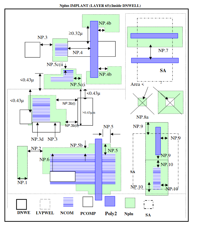
NP.1 |
Width |
0.4 |
NP.2 |
Space |
0.4 |
NP.3a |
Space to PCOMP for PCOMP: (1) Inside Nwell (2) Outside LVPWELL but inside DNWELL |
0.16 |
NP.3b |
Space to PCOMP: For Inside DNWELL, inside LVPWELL: I) For PCOMP overlap by LVPWELL < 0.43μm II) For PCOMP overlap by LVPWELL >= 0.43μm |
0.16 0.08 |
NP.3c |
Space to PCOMP: For Outside DNWELL: I) For PCOMP space to Nwell < 0.43μm II) For PCOMP space to Nwell >= 0.43μm |
0.16 0.08 |
NP.3d |
Min/max space to a butted PCOMP |
0 |
NP.3e |
Space to related PCOMP edge adjacent to a butting edge |
0 |
NP.4a |
Space to related P-channel gate at a butting edge parallel to gate |
0.32 |
NP.4b |
Within 0.32μm of channel, space to P-channel gate extension perpendicular to the direction of Poly2 |
0.22 |
NP.5a |
Overlap of N-channel gate |
0.23 |
NP.5b |
Extension beyond COMP for the COMP (1) inside LVPWELL (2) outside Nwell and DNWELL |
0.16 |
NP.5c |
Extension beyond COMP: For Inside DNWELL: I) For Nplus < 0.43μm from LVPWELL edge for Nwell or DNWELL tap inside DNWELL II) For Nplus >= 0.43μm from LVPWELL edge for Nwell or DNWELL tap inside DNWELL |
0.16 0.02 |
NP.5d |
Extension beyond COMP: For Outside DNWELL, inside Nwell: I) For Nwell overlap of Nplus < 0.43μm II) For Nwell overlap of Nplus >= 0.43μm |
0.16 0.02 |
NP.6 |
Overlap with NCOMP butted to PCOMP |
0.22 |
NP.7 |
Space to unrelated unsalicided Poly2 |
0.18 |
NP.8a |
Minimum Nplus area |
0.35 μm2 |
NP.8b |
Minimum area enclosed by Nplus |
0.35 μm2 |
NP.9 |
Overlap of unsalicided Poly2 |
0.18 |
NP.10 |
Overlap of unsalicided COMP |
0.18 |
NP.11 |
Butting Nplus and PCOMP is forbidden within 0.43μm of Nwell edge (for outside DNWELL) and of LVPWELL edge (for inside DNWELL case). |
|
NP.12 |
Overlap with P-channel poly2 gate extension is forbidden within 0.32μm of P-channel gate |