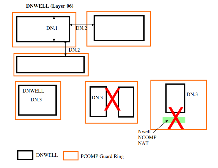
7.2 Dnwell
This layer is defined to put 3.3V and 5V/6V CMOS devices inside deep Nwell for better isolation from substrate noise.
RULE NO. |
DESCRIPTION |
LAYOUT |
Layer |
DN = DNWELL |
|
DN.1 |
Min. DNWELL Width |
1.7 |
DN.2a |
Min. DNWELL Space (Equi-potential), Merge if the space is less than |
2.5 |
DN.2b |
Min. DNWELL Space (Different potential) |
5.42 |
DN.3 |
Each DNWELL shall be directly surrounded by PCOMP guard ring tied to the P-substrate potential. |
|
Note.1 |
Both 3.3V and 5V/6V transistors are not allowed in the same DNWELL. It is a layout Guide for Customer. |