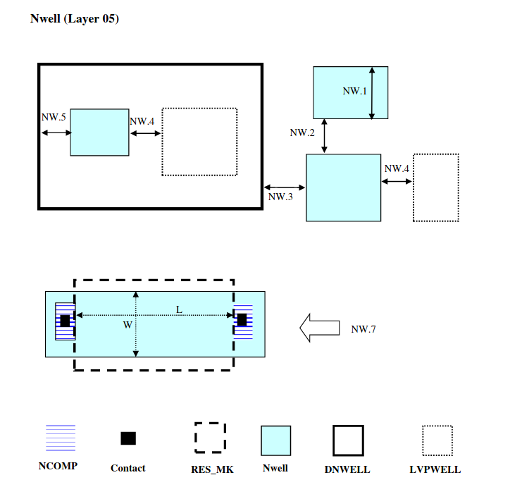
7.4 Nwell
This drawn layer is to define the Nwell for both 3.3V & 5V/6V PMOS transistors. For Nwell as a resistor it can only be used outside DNWELL, as by default all Nwell inside DNWELL will be shorted together through DNWELL.
RULE NO. |
DESCRIPTION |
LAYOUT |
|
Layer |
NW = Nwell |
3.3V |
5V/6V |
NW.1a |
Min. Nwell Width (This is only for litho purpose on the generated area) |
0.86 |
0.86 |
NW.1b |
Min. Nwell Width as a resistor (Outside DNWELL only) |
2 |
2 |
NW.2a |
Min. Nwell Space (Outside DNWELL) [Equi-potential], Merge if the space is less than |
0.6 |
0.74 |
NW.2b |
Min. Nwell Space (Outside DNWELL) [Different potential] |
1.4 |
1.7 |
NW.3 |
Min. Nwell to DNWELL space |
3.1 |
3.1 |
NW.4 |
Min. Nwell to LVPWELL space |
0 |
0 |
NW.5 |
Min. DNWELL enclose Nwell |
0.5 |
0.5 |
NW.6 |
Nwell resistors can only exist outside DNWELL |
||
NW.7* |
If Nwell is used as resistor, it must be covered by RES_MK (for LVS purpose). Width of the resistor determined by Nwell width. Length by COMP to COMP space. RES_MK length shall be coincide with resistor length (Touching COMP each side) and width covering the width of Nwell)” |
Note