8.0 Antenna Ratio Rules
An antenna includes all conducting structures on the same layer and the same electrical node that connect to an active area only via layers below it.
RULE NO. |
DESCRIPTION |
LAYOUT RULE |
Layer |
Poly2, Metal1 to MetalTop |
|
ANT.1 |
Maximum ratio of Poly2 perimeter area to related gate oxide area |
200 |
ANT.2 (1) |
Maximum ratio of Metal1 perimeter area to related gate oxide area |
400 |
ANT.3 (1) |
Maximum ratio of Metal2 perimeter area to related gate oxide area |
400 |
ANT.4 (1) |
Maximum ratio of Metal3 perimeter area to related gate oxide area |
400 |
ANT.5 (1) |
Maximum ratio of Metal4 perimeter area to related gate oxide area |
400 |
ANT.6 (1) |
Maximum ratio of Metal5 perimeter area to related gate oxide area |
400 |
ANT.7 (1) |
Maximum ratio of MetalTop perimeter area to related gate oxide area |
400 |
ANT.8 |
Maximum ratio of contact area to related gate oxide area |
10 |
ANT.9 (1) |
Maximum ratio of Via1 area to related gate oxide area |
20 |
ANT.10 (1) |
Maximum ratio of Via2 area to related gate oxide area |
20 |
ANT.11 (1) |
Maximum ratio of Via3 area to related gate oxide area |
20 |
ANT.12 (1) |
Maximum ratio of Via4 area to related gate oxide area |
20 |
ANT.13 (1) |
Maximum ratio of Via5 area to related gate oxide area |
20 |
ANT.14 |
If MIM is between Metaln and Metal (n+1), Then: Maximum ratio of each of the metal layer (Metal (n+1) to MetalTop) perimeter area to related MIM area (For example, If MIM is between Metal2 and Metal3, then need to check ANT.14 for M3, M4, … MetalTop to its related MIM) |
400 |
ANT.15 |
If MIM is between Metaln and Metal (n+1), then: Maximum ratio of each of Via (Vian to most top Via) area to related MIM area (For example, If MIM is between Metal2 and Metal3, then need to check ANT.15 for V2, V3, … most top Via to its related MIM) |
20 |
Note
Possible repairs to metal antenna nodes, which have a high via count or antenna ratio.
Add an NCOMP/Substrate diode for NMOS gate, PCOMP/Nwell diode for PMOS gate.
Break the metal close to the gate and jog the metal to an upper metal level.
Remedy for Antenna Rule violations:
Connecting antenna diode
RULE NO. |
DESCRIPTION |
LAYOUT RULE |
ANT.16 |
If any of the above antenna ratio rules fails then the antenna diodes shall be connected in a reverse bias mode between the metal line failing antenna ratio (connected to gate poly or MIM cap top plate) and the substrate underneath. For DRC check if Metaln or Vian fails antenna ratio then it shall check whether this Metaln or Vian is directly connected to COMP through lower level metals, vias and contacts or not? Case (a): Connection to COMP is not present: Flag error Case (b): Connection to COMP is present: Then:
Treat Gate area = (thin gate area + MF* (COMP area directly connection that node)) This comp area contained the protection diode and any other drain or source junction connected to this node. MF: stand for multiplying factor, for this case MF=2
DUALGATE) Treat Gate area = (Thick gate area + MF* (COMP area directly connection that node)) This comp area contained the protection diode and any other drain or source junction connected to this node. MF: stand for multiplying factor, for this case MF=15
Treat MIM area = (FuseTop area + MF* (COMP area directly connection that node))(For MIM option-A process) Treat MIM area = (FuseTop area + MF* (COMP area directly connection that node))(For MIM option-B process) This comp area contained the protection diode and any other drain or source junction connected to this node. MF: stand for multiplying factor, for this case MF=15 And check back the validity of antenna ratios as specified in rules ANT.1 to ANT.15. |
(2) Other Possible repairs if the Antenna ratio violate the design rule is break the metal close to the gate and jog the metal to an upper metal level.
ANTENNA RATIO RULES
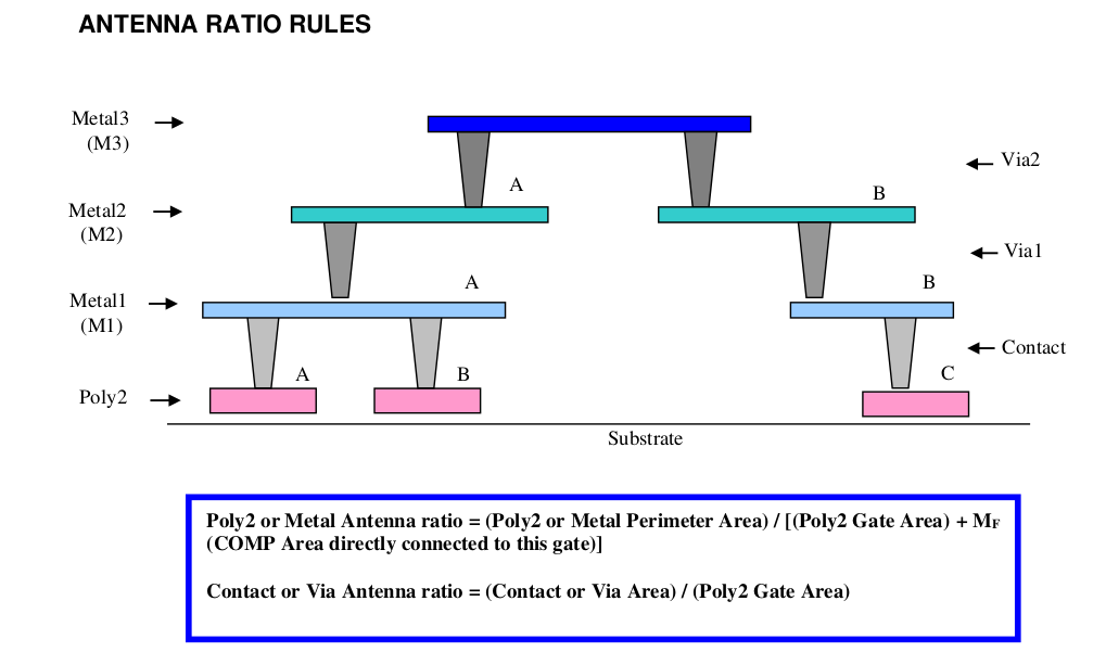
Example:
Illustration on the above antenna ratio calculation: (Terms on the right hand side of the equations below (eg. Metal3) refer to the layout areas of the corresponding structures in the diagram above.)
Poly2/Metal Perimeter Area calculation
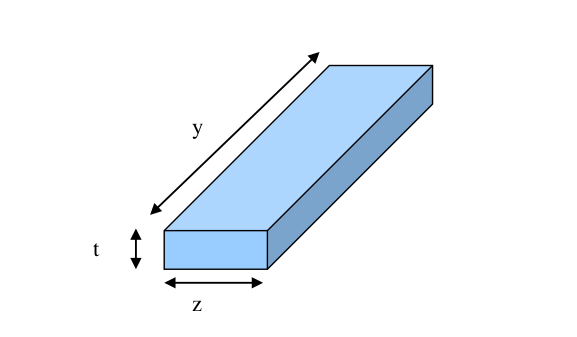
Where
y: Poly2/Metal length
z: Poly2/Metal width
t: Poly2/Metal thickness
Poly2 |
Metal1 |
Metal2 |
Metal3 |
Metal4 |
Metal5 |
MetalTop (6K Å) |
MetalTop.1 (9K Å) |
MetalTop.2 (11K Å) |
MetalTop.3 (30K Å) |
|
t(um) |
0.2um |
0.54um |
0.54um |
0.54um |
0.54um |
0.54um |
0.69um |
0.99um |
1.19um |
3.035um |