7.7 Poly2
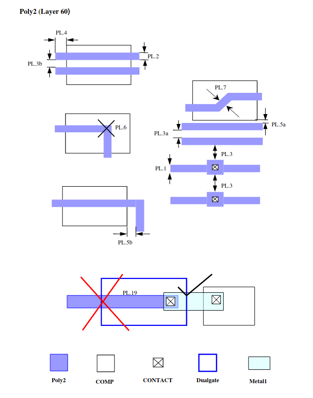
Poly2 defines the Poly2-Gate on CMOS device. The min. channel length for both 3.3V NMOS and PMOS are 0.28um. The min. channel length for 6V NNMOS and PMOS are 0.7um and 0.55um; for 5V are 0.6um and 0.5um.
RULE NO. |
DESCRIPTION |
LAYOUT RULE |
||
Layer |
PL = Poly2 |
3.3V |
5V |
6V |
PL.1 |
Interconnect Width (outside PLFUSE) |
0.18 |
0.2 |
0.2 |
PL.1a |
Interconnect Width (inside PLFUSE) |
0.18 |
0.18 |
0.18 |
PL.2 |
Gate Width (Channel Length) 1 |
0.28 |
0.6/0.5 |
0.7/0.55 |
PL.3a |
Space on COMP Space on Field |
0.24 0.24 |
0.24 0.24 |
0.24 0.24 |
PL.3b* |
Poly2 Space on COMP for low active sheet resistivity (guideline) |
0.26 |
0.4 |
0.4 |
PL.4 |
Extension beyond COMP to form Poly2 end cap |
0.22 |
0.22 |
0.22 |
PL.5a |
Space from field Poly2 to unrelated COMP Spacer from field Poly2 to Guard-ring |
0.1 |
0.3 |
0.3 |
PL.5b |
Space from field Poly2 to related COMP |
0.1 |
0.3 |
0.3 |
PL.6 |
90 deg bends on the COMP are not allowed |
|||
PL.7 |
45 deg bent gate width |
0.3 |
0.7 |
0.7 |
PL.8 |
Poly2 coverage over the entire die shall be >= 14% Dummy poly2 lines must be added to meet the minimum poly2 density requirement. |
|||
PL.9 |
Poly2 inter connect connecting 3.3V and 5V/6V areas (area inside and outside Dualgate) are not allowed. They shall be done though metal lines only. |
|||
PL.10* |
Maximum Poly2 current density |
1mA/um |
1mA/um |
1mA/um |
PL.11 |
V5_Xtor must enclose 5V device |
|||
PL.12 |
V5_Xtor enclose 5V Comp |
NA |
0 |
NA |
Note
Note
The min. channel length for 6V NNMOS and PMOS are 0.7um and 0.55um; for 5V are 0.6um and 0.5um.
Parasitic capacitance needs to be considered when adding dummy poly2. Customer has the option to use GlobalFoundries’s dummy poly2 generation rule. In this case, customer needs to mark out areas of circuit which are sensitive to parasitic capacitance and do not want dummy poly2 fill generated. Customer need to separate circuit Metal1 and Metal2 from dummy metal in order that dummy poly2 can be generated beneath dummy metal. Refer to 4.1 for layer name