10.12.2 10V LDPMOS rules
This is to define P type asymmetrical 10V LDMOS device (LDPMOS) Below is a summary table as how to identify the device.
Items |
Layers or Logic operations for identifying the device and its nodes |
LDPMOS |
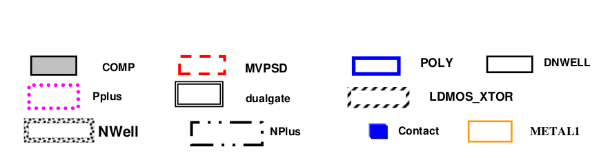
Device under LDMOS_XTOR with Dualgate and COMP, Poly2, MVPSD |
LDPMOS Drain |
MVPSD |
LDPMOS Source |
((Pplus AND COMP) Interact (((Poly2 AND Dualgate) AND LDMOS_XTOR) AND MVPSD)) NOT Poly2 |
LDPMOS Channel Length |
MVPSD space to POLY2 edge in COMP |
LDPMOS Channel Width |
LDPMOS COMP width intersecting with (((POLY2 AND Dualgate) AND (LDMOS_XTOR Interact MVPSD)) |
Rule NO |
Description |
Layout Rule |
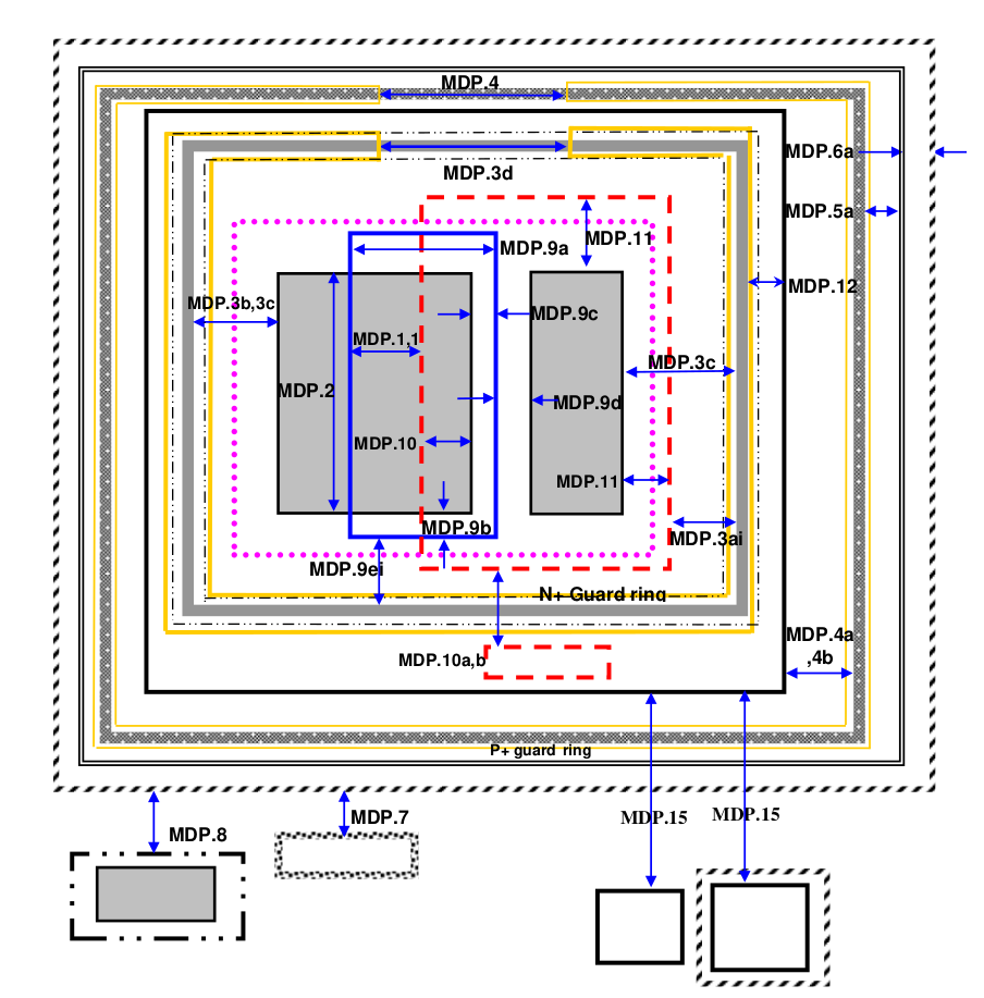
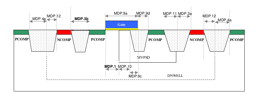
MDP.1 |
Minimum transistor channel length |
0.6 |
MDP.1a |
Max transistor channel length |
20 |
MDP.2 |
Minimum transistor channel width |
4 |
MDP.3 |
Each LDPMOS shall be surrounded by non-broken Nplus guard ring inside DNWELL. Nplus guard ring shall be connected to the highest potential. It is better to put wider than minimum guard ring for latch-up prevention if LDNMOS and LDPMOS are adjacent to each other (refer to latch-up guidelines in section 14.5.4). |
|
MDP.3ai |
Min NCOMP (Nplus AND COMP) space to MVPSD (source and body tap non-butted) NCOMP (Nplus AND COMP) intercept with MVPSD is not allowed |
1 |
MDP.3aii |
Min NCOMP (Nplus AND COMP) space to MVPSD (source and body tap butted) NCOMP (Nplus AND COMP) intercept with MVPSD is not allowed |
0.92 |
MDP.3b |
Min NCOMP (Nplus AND COMP) space to PCOMP in DNWELL (Pplus AND COMP AND DNWELL). Use butted source and DNWELL contacts otherwise and that is best for Latch-up immunity as well |
0.4 |
MDP.3c |
Maximum distance of the nearest edge of the DNWELL tab (NCOMP inside DNWELL) from PCOMP edge (PCOMP inside DNWELL) |
15 |
MDP.3d |
The metal connection for the Nplus guard ring recommended to be continuous, The maximum gap between this metal if broken Note: To put maximum number of contact under metal for better manufacturability and reliability |
10 |
MDP.4 |
DNWELL covering LDPMOS shall be surrounded by non broken Pplus guard The metal connection for the Pplus guard ring recommended to be continuous, The maximum gap between this metal if broken. Note: To put maximum number of contact under metal for better manufacturability and Reliability |
10 |
MDP.4a |
Min PCOMP (Pplus AND COMP) space to DNWELL |
2.5 |
MDP.4b |
Maximum distance of the nearest edge of the DNWELL from the PCOMP Guard ring outside DNWELL |
15 |
MDP.5 |
Each LDPMOS shall be covered by Dualgate layer, |
|
MDP.5a |
Minimum Dualgate enclose Plus guarding ring PCOMP (Pplus AND COMP) |
0.5 |
MDP.6 |
Each LDPMOS shall be covered by LDMOS_XTOR (GDS#226) layer |
|
MDP.6a |
Minimum LDMOS_XTOR enclose Dualgate |
0 |
MDP.7 |
Minimum LDMOS_XTOR (GDS#226) layer space to Nwell outside LDMOS_XTOR |
2 |
MDP.8 |
Minimum LDMOS_XTOR (GDS#226) layer space to NCOMP (Nplus AND COMP) outside LDMOS_XTOR (GDS#226) |
1.5 |
MDP.9 |
POLY2 rules |
|
MDP.9a |
Min LDPMOS POLY2 width (POLY2 inside DNWELL AND LDMOS_XTOR (GDS#226)) |
1.2 |
MDP.9b |
Min POLY2 extension beyond COMP in the width direction of the transistor (other than the LDMOS drain direction) |
0.4 |
MDP.9c |
Min/Max POLY2 extension beyond COMP on the field towards LDPMOS drain (MVPSD AND COMP AND Pplus NOT POLY2) direction |
0.2 |
MDP.9d |
Min/Max POLY2 on field to LDPMOS drain COMP (MVPSD AND COMP AND Pplus NOT POLY2) space |
0.16 |
MDP.9ei |
Min LDMPOS gate Poly2 space to Nplus guardring (source and body tap non- Butted) |
0.4 |
MDP.9eii |
Min LDMPOS gate Poly2 space to Nplus guardring (source and body tap butted) |
0.32 |
MDP.9f |
Poly2 interconnect is not allowed in LDPMOS region (LDMOS_XTOR marked Region) |
|
MDP.10 |
Min/Max MVPSD overlap onto the channel (LDMOS_XTOR AND COMP AND POLY2 AND Pplus) |
0.4 |
MDP.10a |
Min MVPSD space within LDMOS_XTOR marking [diff potential] |
2 |
MDP.10b |
Min MVPSD space [same potential] Merge if space less than 1um |
1 |
MDP.11 |
Min MVPSD enclosing PCOMP in the drain (MVPSD AND COMP NOT POLY2) direction and in the direction along the transistor width. |
0.8 |
MDP.12 |
Min DNWELL enclose Nplus guard ring (NCOMP) |
0.66 |
MDP.13 |
Wide width transistor can be used with multi finger with following rules |
|
MDP.13a |
Max single finger width |
50 |
MDP.13b |
Layout shall have alternative source & drain |
|
MDP.13c |
Both sides of the transistor shall be terminated by source |
|
MDP.14 |
Others unlisted layer like Nplus, Pplus, Nwell, Contact, Metal, VIA, shall follow MV rules listed in section 7.0 |
|
MDP.15 |
Min “DNWELL enclosing MVPSD” to any DNWELL spacing |
6 |
MDP.16a |
Min LDPMOS drain COMP width |
0.22 |
MDP.16b |
Min LDPMOS drain COMP enclose contact |
0 |
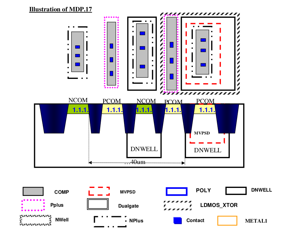
MDP.17 |
Between “MVPSD Inside DNWELL covered by LDMOS_XTOR” and NCOMP (outside DNWELL and outside Nwell) when spacing between them is less than 40um
DF.4b, DF.18, and MDP.15.
|