10.12.1 10V LDNMOS rules
This is to define N type asymmetrical 10V LDMOS device (LDNMOS). Below is a summary table as how to identify the device. All this kind of device’s well share the same potential with P-substrate.
Items |
Layers or Logic operations for identifying the device and its nodes |
LDNMOS |
Device under LDMOS_XTOR with Dualgate and COMP, Poly2, MVSD |
LDNMOS Drain |
MVSD |
LDNMOS Source |
((Nplus AND COMP) Interact (((Poly2 AND Dualgate) AND LDMOS_XTOR) AND MVSD)) NOT Poly2 |
LDNMOS Channel Length |
MVSD space to POLY2 edge in COMP |
LDNMOS Channel Width |
LDNMOS COMP width intersecting with (((POLY2 AND Dualgate) AND (LDMOS_XTOR Interact MVSD))” |
Rule NO |
Description |
Layout Rule |
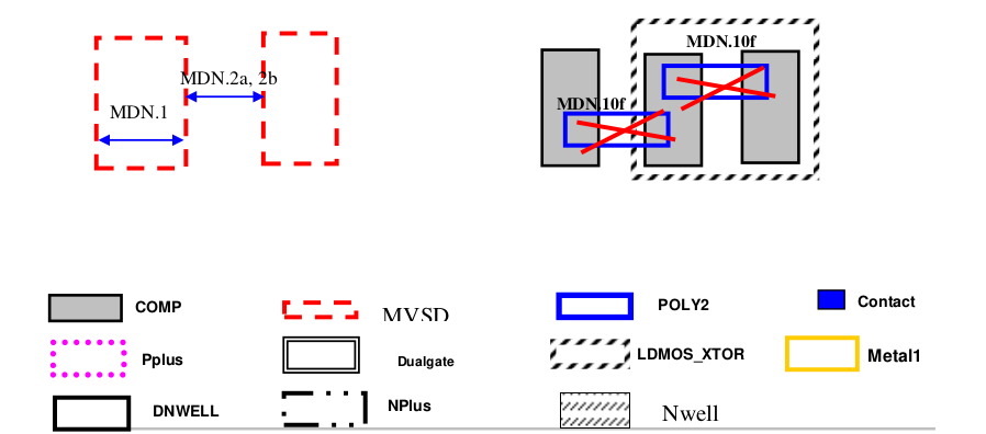
MDN.1 |
Min MVSD width (for litho purpose) |
1 |
MDN.2a |
Min MVSD space [Same Potential] |
1 |
MDN.2b |
Min MVSD space [Diff Potential] |
2 |
MDN.3a |
Min transistor channel length |
0.6 |
MDN.3b |
Max transistor channel length |
20 |
MDN.4a |
Min transistor channel width |
4 |
MDN.4b |
Max transistor channel width |
50 |
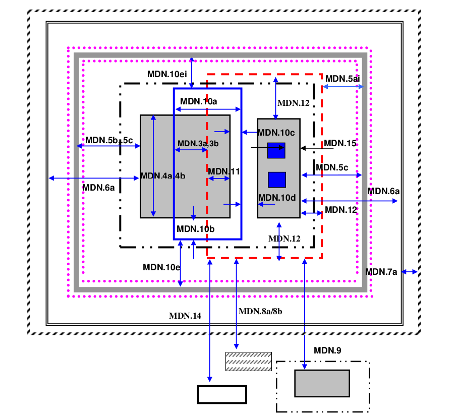
MDN.5ai |
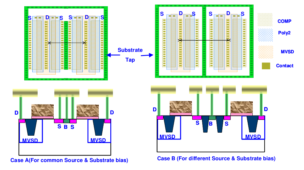
Min PCOMP (Pplus AND COMP) space to LDNMOS Drain MVSD (source and body tap non-butted) PCOMP (Pplus AND COMP) intercept with LDNMOS Drain MVSD is not allowed |
1 |
MDN.5aii |
Min PCOMP (Pplus AND COMP) space to LDNMOS Drain MVSD (source and body tap butted) PCOMP (Pplus AND COMP) intercept with LDNMOS Drain MVSD is not allowed |
0.92 |
MDN.5b |
Min PCOMP (Pplus AND COMP) space to LDNMOS Source (Nplus AND COMP) Use butted source and p-substrate tab otherwise and that is good for Latch-up immunity as well. |
0.4 |
MDN.5c |
Maximum distance of the nearest edge of the substrate tab from NCOMP edge |
15 |
MDN.6 |
ALL LDNMOS shall be covered by Dualgate layer |
|
MDN.6a |
Min Dualgate enclose NCOMP |
0.5 |
MDN.7 |
Each LDNMOS shall be covered by LDMOS_XTOR (GDS#226) mark layer |
|
MDN.7a |
Min LDMOS_XTOR enclose Dualgate |
0 |
MDN.8a |
Min LDNMOS drain MVSD space to any other equal potential Nwell space |
1 |
MDN.8b |
Min LDNMOS drain MVSD space to any other different potential Nwell space |
2 |
MDN.9 |
Min LDNMOS drain MVSD space to NCOMP (Nplus AND COMP) outside LDNMOS drain MVSD |
4 |
MDN.10 |
POLY2 rules |
|
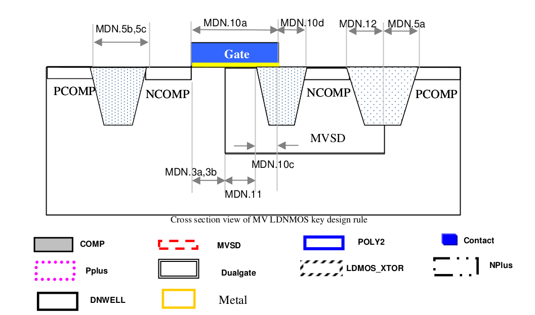
MDN.10a |
Min LDNMOS POLY2 width |
1.2 |
MDN.10b |
Min POLY2 extension beyond COMP in the width direction of the transistor (other than the LDNMOS drain direction) |
0.4 |
MDN.10c |
Min/Max POLY2 extension beyond COMP on the field towards LDNMOS drain COMP Direction |
0.2 |
MDN.10d |
Min/Max POLY2 on field space to LDNMOS drain COMP |
0.16 |
MDN.10ei |
Min POLY2 space to Psub tap (source and body tap non-butted) |
0.4 |
MDN.10eii |
Min POLY2 space to Psub tap (source and body tap butted) |
0.32 |
MDN.10f |
Poly2 interconnect in HV region (LDMOS_XTOR marked region) not allowed. Also, any Poly2 interconnect with “poly2 to substrate” potential greater than 6V is not Allowed) |
|
MDN.11 |
Min/Max MVSD overlap channel COMP ((((LDMOS_XTOR AND MVSD) AND COMP) AND POLY2) AND Nplus) |
0.4 |
MDN.12 |
Min MVSD enclose NCOMP in the LDNMOS drain and in the direction along the transistor width. |
0.5 |
MDN.13 |
Wide width transistor can be used with multi finger type with following rules: |
|
MDN.13a |
Max single finger width |
50 |
MDN.13b |
Layout shall have alternative source & drain |
|
MDN.13c |
Both sides of the transistor shall be terminated by source |
|
MDN.13d |
Every two poly fingers shall be surrounded by a P-sub guard ring. (Exclude the case when each LDNMOS transistor have full width butting to well tap) |
|
MDN.14 |
Min MVSD space to any DNWELL |
6 |
MDN.15a |
Min LDNMOS drain COMP width |
0.22 |
MDN.15b |
Min LDNMOS drain COMP enclose contact |
0 |
MDN.16 |
Others unlisted layer like Nplus, Pplus, CONTACT, Metal, VIA, shall follow MV rules listed in section 7.0 |
|
MDN.17 |
It is recommended to surround the LDNMOS transistor with non-broken Psub guard ring Guideline to improve the latch up immunity. |
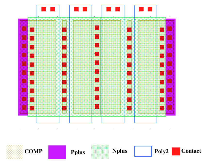
Rule MDN.13d when each LDNMOS transistor has full width butting to well tap
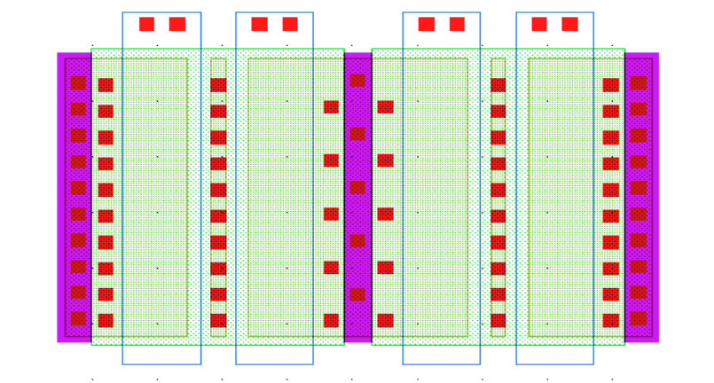
In below example, not every transistor has full width butting to well tap, it violate rule MDN.13d