10.10 OTP_MK Mark Layer
This layer is used to mark 3.3V OTP cells. OTP cells with this marking layer should follow below specific rules which is different from 3.3V/(5V)6V rules.
RULE NO. |
DESCRIPTION |
LAYOUT RULE |
|
3.3V OTP |
5V OTP (1) |
||
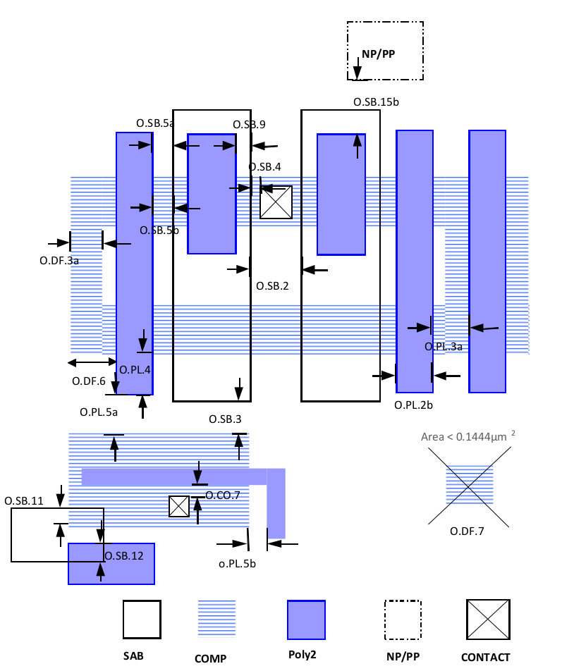
O.DF.3a |
Min. COMP Space. P-substrate tap (PCOMP outside NWELL) can be butted for different voltage devices as the potential is same |
0.24 |
0.24 |
O.DF.6 |
Min. COMP extend beyond poly2 (it also means source/drain overhang) |
0.22 |
0.22 |
O.DF.9 |
Min. COMP area (um2) |
0.1444 |
0.1444 |
O.PL.2 |
Min. poly2 width |
0.22 |
0.22 |
O.PL.3a |
Min. poly2 Space on COMP |
0.18 |
0.18 |
O.PL.4 |
Min. extension beyond COMP to form Poly2 end cap |
0.14 |
0.14 |
*O.PL.5a |
Min. space from field Poly2 to unrelated COMP. Min. space from field Poly2 to Guard-ring. |
0 |
0 |
*O.PL.5b |
Min. space from field Poly2 to related COMP |
0 |
0 |
O.SB.2 |
Min. salicide Block Space |
0.28 |
0.28 |
O.SB.3 |
Min. space from salicide block to unrelated COMP |
0.09 |
0.09 |
O.SB.4 |
Min. space from salicide block to contact |
0.03 |
0.03 |
*O.SB.5a |
Min. space from salicide block to unrelated Poly2 on field |
0 |
0 |
O.SB.5b |
Min. space from salicide block to unrelated Poly2 on COMP |
0.1 |
0* |
O.SB.9 |
Min. salicide block extension beyond unsalicided Poly2 |
0.1 |
0.1 |
O.SB.11 |
Min. salicide block overlap with COMP |
0.04 |
0.04 |
*O.SB.12 |
Min. salicide block overlap with Poly2 |
0 |
0 |
O.SB.13 |
Min. area of silicide block (um2) |
1.488 |
2 |
*O.SB.15b |
Min. space from unsalicided Poly2 to unrelated Nplus/Pplus along Poly2 Line |
0 |
0 |
O.CO.7 |
Min. space from COMP contact to Poly2 on COMP |
0.13 |
0.13 |
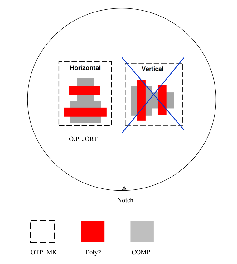
O.PL.ORT |
Orientation-restricted gates must have the gate width aligned along the X-axis (poly line running horizontally) in reference to wafer notch down |
DRC |
NA |
Note
* Rules allowed minimum overlap and spacing are 0, so DRC deck will not check those rules 1. Rule of 5V OTP is set by utilizing “V5_XTOR” and “OTP_MK” marking layer