10.8 Design Rules for Dummy Exclude layers (NDMY and PMNDMY)
This section describes the design rules for drawing dummy exclude layers “NDMY” for excluding “Dummy COMP” and “PMNDMY” for excluding “Dummy Poly” and “Dummy metal” in that area. There shall be intended minimal use of NDMY layer in active transistor areas so as to provide better STI process margins and active transistor performance.
RULE NO. |
DESCRIPTION |
LAYOUT RULE |
DE.1* |
Dummy COMP exclude and dummy poly/metal exclude layers shall be drawn only if necessary (for example for certain critical RF circuit area where RF coupling is critical). Other wise in normal analog and digital active circuits, the presence of “dummy COMP” Around it rather maintains the better Ioff performance of the transistors and junctions. |
|
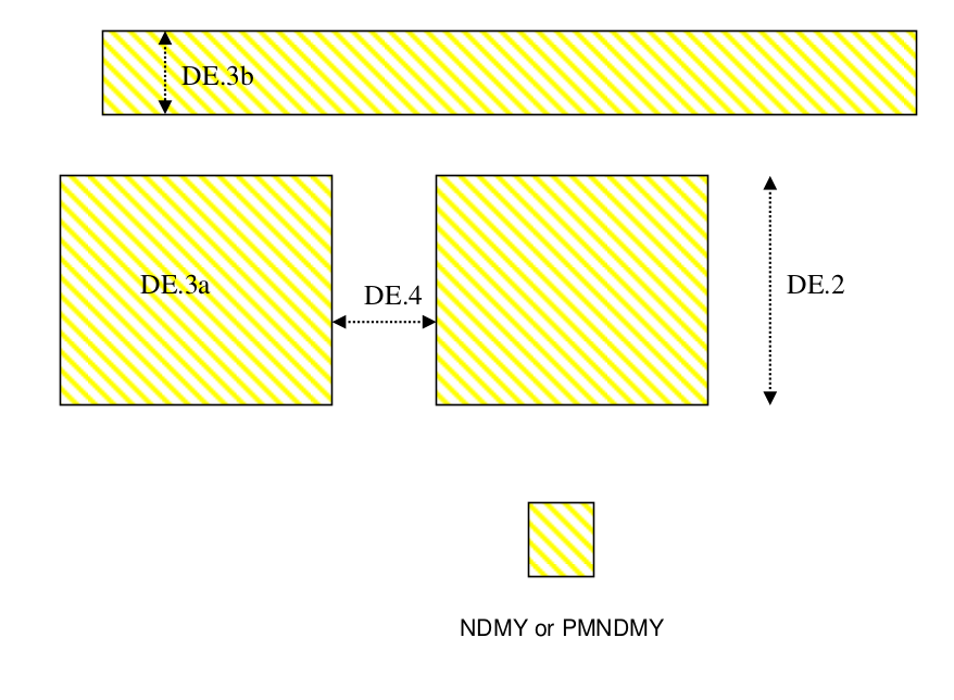
DE.2 |
Minimum NDMY or PMNDMY size (x or y dimension in um) |
0.8 |
DE.3 |
|
15000 |
|
80 |
|
DE.4 |
Minimum NDMY to NDMY space (Merge if space is less). |
20 |
Note