10.6.1 Devices required to be laid out as matched pair
Most of the time, the following are the type of devices required to be drawn for a good matched pair
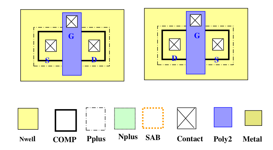
(1) MOS Transistors
NMOS Matched pair: Two NMOS of same type (same operating voltage and process layers) required to be matched in electrical characteristics. (S: Source, D: Drain, G: Gate)
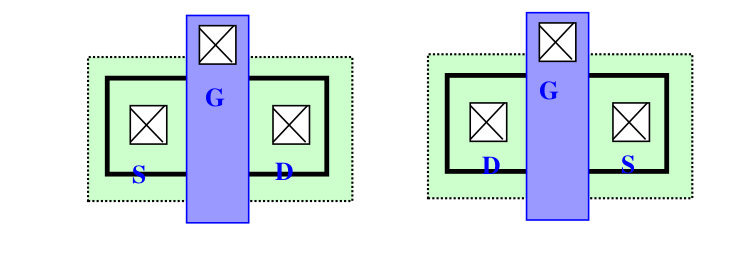
PMOS Matched pair: Two PMOS of same type (same operating voltage and process layers) required to be matched in electrical characteristics. (S: Source, D: Drain, G: Gate)
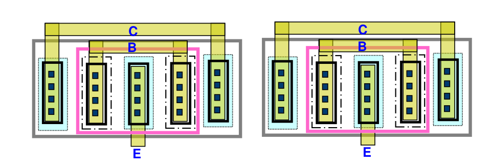
(2) BJT Transistors
Two BJT transistors (NPNs or PNPs) of same type (same operating voltage and process layers) required to be matched in electrical characteristics: (E: Emitter, B: Base, C: Collector).
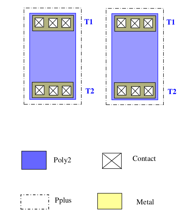
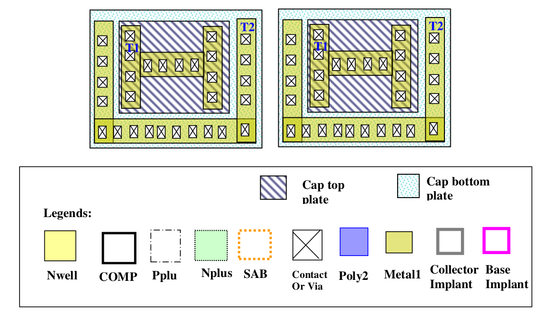
(3) Capacitors
Two identical (same operating voltage and process layers) capacitor (e.g MIM Caps) required to be matched in electrical characteristics. (T1: Capacitor top plate terminal, T2: capacitor’s bottom plate terminal).
(4) Resistors
Two identical (same operating voltage and process layers) resistors (e.g Poly resistors) required to be matched in electrical characteristics. (T1: resistors one terminal, T2: Resistor’s other terminal).