9.4.3 Solder Bump Pad design guidelines
This section contains the bumping design guidelines for flip chip applications
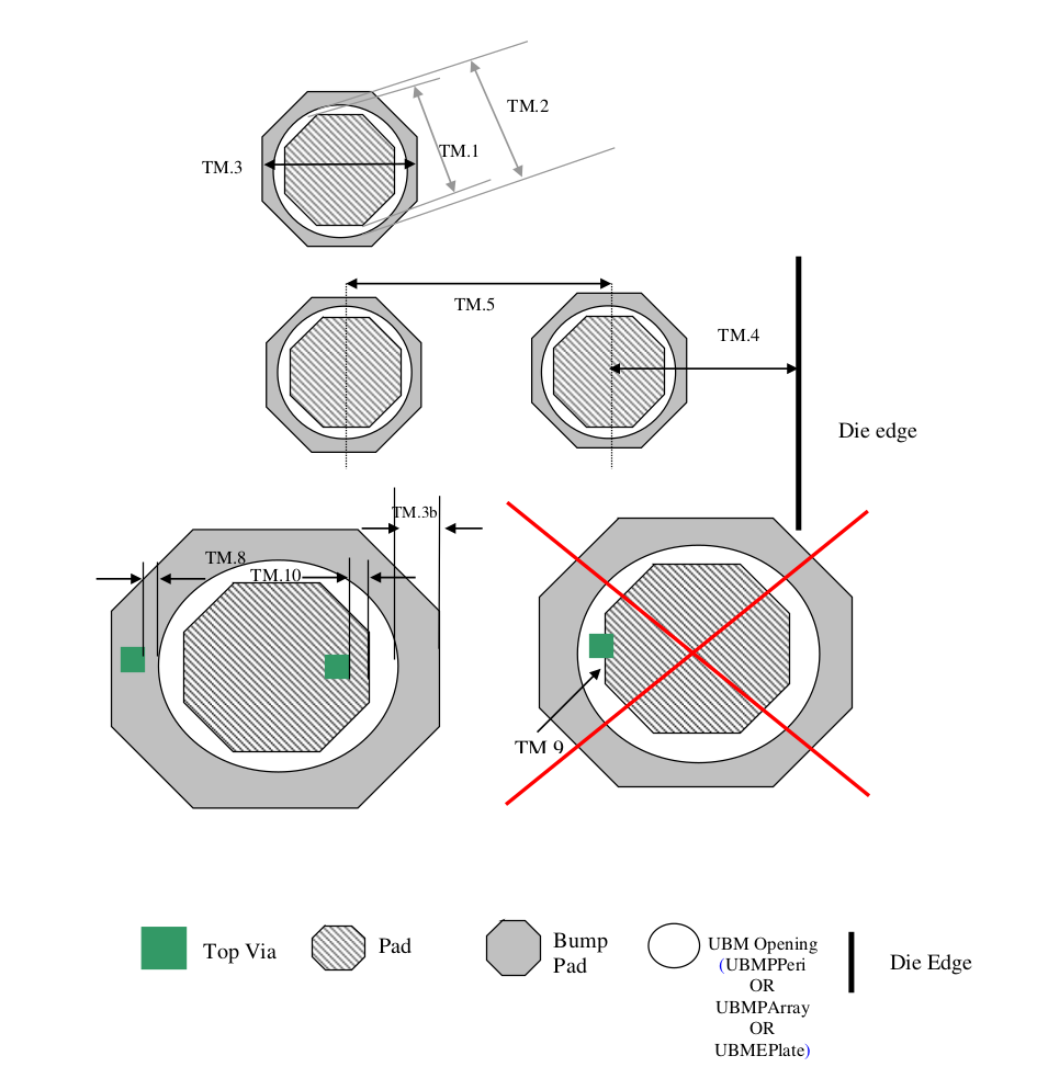
Top Metal (Al)
NO. |
DESCRIPTION |
LAYOUT RULE |
TM.1 |
Passivation Opening (Pad mask) |
A |
TM.1a |
Min Passivation Opening |
40 |
TM.2* |
UBM Opening |
A+20 |
TM.2a |
Min UBM Opening (defined by the layers UBMPPeri or UBMPArray or UBMEPlate layers depending upon the process) |
60 |
TM.3 |
Bump Pad (Top metal in this case) |
A+32 |
TM.3a |
Min Bump Pad |
72 |
TM. 3b* |
Bump Pad larger then UBM Opening |
6 / per side |
TM. 4 |
Space from centre of Pad to Die Edge (Outer edge of GUARD_RING_MK marking) |
90 |
TM. 5 |
Min allowable bump pitch |
>= 70 + (1.3*TM.2) |
TM.6 |
Pad without UBM layers is not allowed except the Pad under PROBE_MK marking. |
Not allowed |
TM.7 |
Shape of the Pad shall be at least octagonal (or more closer to circular) except the Pad under PROBE_MK marking. |
DRC check |
TM.8 |
Space from edge of top via to the edge of UBM opening |
2 |
TM.9 |
Partially overlap of top via with passivation opening is not allowed |
DRC check |
TM.10 |
Space from edge of top via to the edge of passivation opening |
2 |
Note
* Use tolerance of 0.2um for DRC check.