9.3 Circuit-Under-Pad (CUP) Rules
Active circuits are allowed when ball-type wire-bonding process is used and when bumping/flip chip technology is used. No circuit under pad is allowed when wedge-type wire-bonding process is used. The following additional rules apply to designs when active circuits are used under the pad.
Note
It is strongly recommended to optimize the bonding parameters (bond force, time and power) when using CUP for the first time in the design. Bonding parameters used for pads with no circuits underneath the pad may not necessarily be optimized for CUP application. After performing a design of experiments with bonding parameters, wire-pull and ball-shear tests should be performed to ensure mechanical stability of CUP bond pads (no lift-off or cratering of balls for optimized bonding parameters). Cross section of pad area should be taken to make sure that there is no crack underneath the bond pad. By following the design rules described in this section, robust CUP designs can be achieved but because bonding parameters may differ from one assembly house to the other, some optimization may be necessary for CUP bond pads when used for the first time.
Rule NO. |
DESCRIPTION |
Ball type Wire bond |
Solder bump/Gold bump |
CUP.1 |
All FEOL are allowed to be below Pad region (except the items stated in CUP.4). |
Per Design Manual |
Per Design Manual |
CUP.1a |
CUP is not allowed for Wedge-type Wire bond case. |
||
CUP.2 |
Minimum width of the metal line used for bond pads |
1 |
NA |
CUP.3 |
Minimum space of the metal line used for bond pads (slots) |
1 |
NA |
CUP.4* (1) |
Circuits currently not allowed under bond pad are: - Devices sensitive to strain (eg: silicon band-gap references) - Matched pair devices like transistors, resistors and capacitors For precision analog application. - All RF components |
Guideline |
Guideline |
CUP.5 |
Top vias directly underneath the pad opening |
Not Allowed |
NA |
CUP.6 |
However it is good to have a ring of top vias connected around the pad opening to MetalTop-1 with min top via space to pad opening: |
0.5 |
NA |
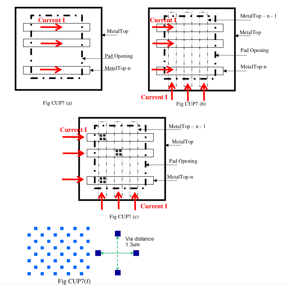
CUP.7 |
a) Guideline: Metals underneath pad shall be in the form of stripes which Should be aligned parallel to the expected current flow during normal operation and ESD condition. Refer Fig.CUP7(a) |
||
b) Guideline*: If orthogonal current flow is required crosshatched Metal grids with similar line and space may be used. Refer Fig.CUP7(b) |
|||
c) Vias shall be in the form of cluster or arrays (<=3x3). Sea of Via (>3x3 array) is not allowed. Refer Fig.CUP7(c) |
|||
d) Min via space in via arrays |
0.3 |
NA |
|
e) Min space between via arrays |
0.5 |
NA |
|
f) Guideline: Individual top vias (Space = 1.3um) may be used under pad open area. Refer Fig.CUP7(f) |
|||
CUP.8 |
Top_Via-1 (2) directly underneath the Pad mask |
Not Allowed |
NA |
CUP.8a |
Top_Via-1 (2) under the top metal with min top_Via-1 (2) space to pad opening |
0.5 |
NA |
CUP.9 |
1LM, 2LM and 3LM process with CUP. |
Not Allowed |
NA |
Note
Note
This rule cannot be checked by DRC deck; this is just a guideline to the layout engineer to take care.
Top_Via-1: is the one level lower via than top most via, for 6 layer metal product, Top_Via-1 is Via4, for 4Layer metal product, Top_Via-1 is Via2.