13.1 Design rules for Dummy COMP creation.
Dummy COMP rules are required to enable planarization process for shallow trench isolation. Non-functional dummy COMP features are added in large open areas without active features. They are necessary around an isolated active device to minimize STI elevation difference in isolated and dense areas.
It is to be noted that “dummy COMP” shall be drawn in certain systematic way, however dummy features and spacing being much bigger than the lithography and etch capability, the rules are categorized in two category, one for the way of drawing and the other for the DRC (Design rule check) purpose. So, for DRC deck will have only rules marked as “for DRC check” as indicated in last column below. The rules indicated as “for DRC” would imply that they shall be taken care during drawing as well as checked the DRC there after.
RULE NO. |
DESCRIPTION |
LAYOUT RULE |
For Drawing OR DRC Check |
Layer |
DCF-Dummy COMP Fill |
||
Use “NDMY” mark layer to exclude dummy COMP generation in certain critical High frequency/RF circuit areas. |
– |
– |
|
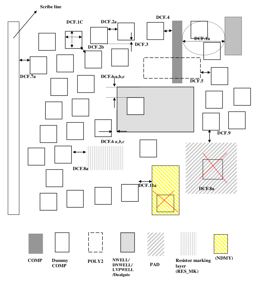
DCF.1a |
All area between active polygons (COMP) (with spacing greater than equal to this rule) must be filled with “Dummy COMP” except area marked by NDMY, RES_MK, Pad and IND_MK, as well as the Region define by DCF.6a, 6b, 6c, 6d, 6e. Use rules DCF.1c to DCF.13 to drawn “Dummy COMP” |
20 |
For DRC |
DCF.1b |
Minimum global density for active layers (COMP+ Dummy COMP) Local density is governed by DCF.1a , DE.3 and DE.4 |
25% |
For DRC |
DCF.1c |
A staggered array of dummy COMP 5 umX5 um squares is created to cover the prime die (1), frame, SLM Etest patterns and SLM reliability test patterns. |
5X5 |
DRC check for |
DCF.1d |
Maximum global density for active layers (COMP+ Dummy COMP) |
70% |
For DRC |
DCF.2a* |
Min/Max Adjacent placement Space between dummy COMP cells |
3 |
For Drawing |
DCF.2b |
Resulted minimum space between Dummy active in all directions (for DRC check) |
1.9 |
For DRC |
DCF.3* |
Stagger both X and Y direction |
1.6 |
For Drawing |
DCF.4 |
Space from dummy COMP to COMP (circuit COMP). |
3.5 |
For DRC |
DCF.5 |
Space from dummy COMP to poly2 |
1.5 |
For DRC |
DCF.6a |
Space from dummy COMP to Nwell boundary |
1.3 |
For DRC |
DCF.6b |
Space from dummy COMP to DNWELL boundary |
4 |
For DRC |
DCF.6c |
Space from dummy COMP to LVPWELL boundary |
1.3 |
For DRC |
DCF.6d |
Space from dummy COMP to Dualgate boundary |
1.3 |
For DRC |
DCF.7a* |
Space from dummy COMP in prime die including guard ring to the scribe line |
26 |
For DRC |
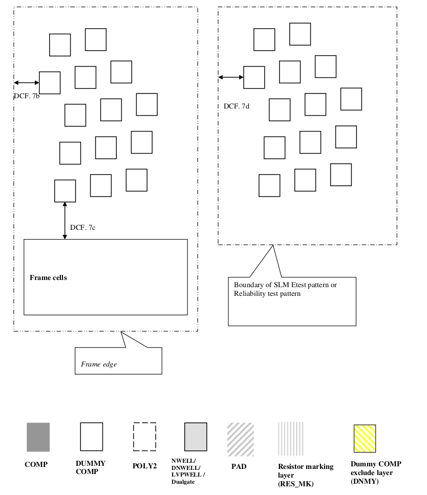
DCF.7b* |
Space from dummy COMP in frame to edge of frame (valid only for scribe lines) |
6 |
For DRC |
DCF.7c* |
Space from dummy COMP in frame to any frame cell except non-ET (valid only for scribe line structures) |
10 |
For Drawing |
DCF.7d* |
Space from dummy COMP in SLM Etest patterns or SLM reliability test patterns to the boundary of test patterns (valid only for scribe line Structures) |
6 |
For DRC |
DCF.8a |
Space from dummy COMP to Resistor marking layer (RES_MK). Dummy COMP should not exit under RES_MK |
3.5 |
For DRC |
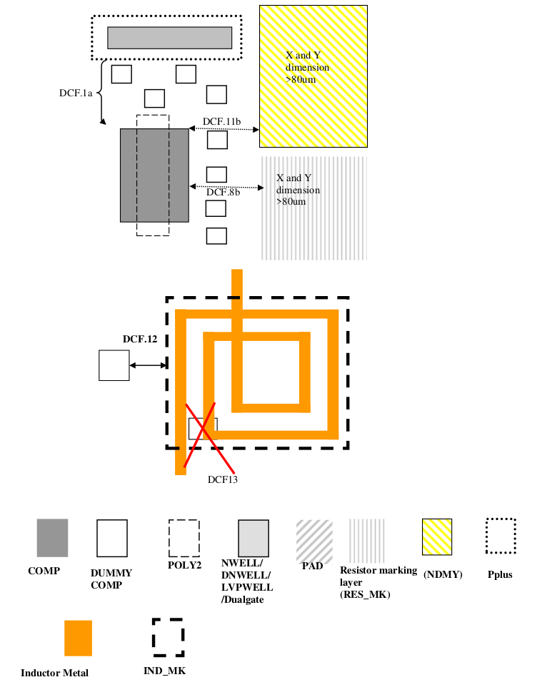
DCF.8b |
There must be at least one row of dummy COMP (or substrate tie) between RES_MK layer and the transistor channel active if RES_MK layer’s both side (x and y) dimensions are greater than: |
80 |
For DRC |
DCF.9* |
Space from dummy COMP to Pad (Just a guideline for RF circuits) |
7 |
Guideline only,no DRC |
DCF.10* |
Remove truncated dummy squares (Truncated Dummy COMP shall not exist) |
– |
For DRC |
DCF.11a |
Dummy COMP cannot exit under “NDMY” marking layer and space from dummy COMP to dummy COMP excluding layer (NDMY) (2) |
3.5 |
For DRC |
DCF.11b |
There must be at least one row of dummy COMP (or substrate tie) between NDMY layer and the transistor channel active if NDMY layer’s both side (x and y) dimensions are greater than: |
80 |
For DRC |
DCF.12 |
Minimum dummy COMP space to IND_MK layer |
3 |
For DRC |
DCF.13 |
Dummy COMP should not exist under IND_MK layer There must be at least one row of dummy COMP (or substrate tie) between IND_MK layer and the transistor channel active if IND_MK layer’s both side (x and y) dimensions are greater than: |
80 |
Note
The prime die, frame, SLM Etest patterns and SLM reliability test patterns will have the same dummy COMP generation algorithm.
Use dummy COMP exclude layer for all non-ET patterns in the frame