14.4.4 Design Guidelines for 5V/6V HV SAB PMOS Device
When using HV PMOSFET for ESD protection devices, it shall be marked by ESD_MK mark layer. The following layout guidelines are recommended.
RULE NO. |
DESCRIPTION |
RULE |
HVPESD.1 |
|
0 |
HVPESD.2* |
Poly Channel-length for each finger in multi-finger transistors must be same |
|
G_HVPESD.3 |
Min. channel length for each finger (Recommended) |
0.7 |
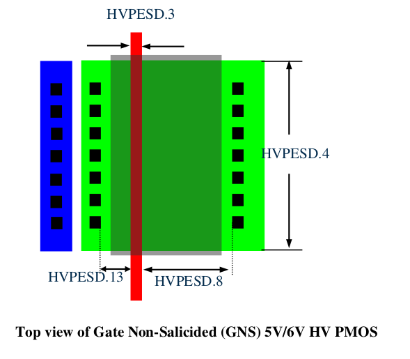
G.HVPESD.4 (a)** |
Recommended finger width for each finger |
25 |
HVPESD.4 (b) |
Min. finger width for each finger |
20 |
HVPESD.4 (c) |
Max. finger width for each finger |
60 |
G.HVPESD.5 (a)** |
Recommended number of fingers share one pick-up ring in multi-finger transistors. |
18 |
HVPESD.5(b) |
Max. number of fingers share one pick-up ring in multi- finger transistors |
24 |
G.HVPESD.6(a)** |
Recommended total finger width |
450 |
HVPESD.6(b) |
Min. total finger width |
300 |
HVPESD.6(c) |
Max. total finger width |
720 |
HVPESD.7 |
SAB should cover drain and source and overlap gate or cover drain only with rule HVPESD.7(a) partly overlap poly Gate |
|
HVPESD.7 (a) |
Min/max SAB overlap Poly gate |
0.05 |
G.HVPESD.8 (a)** |
Recommeded at least one or nearest drain contact to gate edge space (DCGS) |
3 |
HVPESD.8(b) |
Min. drain contact to gate edge space (DCGS) |
1 |
HVPESD.8(c) |
Max. at least one or nearest drain contact to gate edge space (DCGS) |
4 |
G_HVPESD.10 |
Recommended NField well tap COMP to active COMP space in channel length direction. |
2 |
HVPESD.11 |
Source COMP must enclose by LVS_Source |
0 |
HVPESD.12 |
LVS_Source must butt to Poly edge |
0 |
G.HVPESD.13** |
Recommended at least one or nearest source contact to gate edge space (SCGS) when SAB cover drain-source over poly gate |
0.5 |
HVPESD.13(a) |
Min. source contact to gate edge space (SCGS) when SAB cover drain-source over poly gate |
0.15 |
HVPESD.13(b) |
Max. at least one or nearest source contact to gate edge space (SCGS) when SAB cover drain-source over poly gate |
1 |
COHVPESD.7 |
Recommended/max. salicided block edge to at least one or nearest contact (CA) |
0.22 |
COHVPESD.7(a) |
Min. salicided block edge to contact (CA) |
0.15 |