14.3.2 I/O Latch-up Related Rules and Guidelines
I/O regions are more susceptible to latch-up because of over voltage (P+ COMP potential exceeding Vdd) and under voltage (N+ COMP potential below Ground) conditions that may occur there. The most latch-up-prone areas are around the diffusions directly connected to a pad driving an off-chip load. The following design guidelines will help prevent latch-up in I/O area.
Use marking layer “Latchup_MK” coinciding with the boundary of the diffusion directly connected to the I/O pad and other diffusions which designer want to applied I/O rules for robust latchup immunity. Examples of such diffusions are:
diodes that can be potentially forward biased, such as ESD diodes;
Nodes that experience significant over voltage with respect to Vdd or under voltage with respect to Vss.
Those pads connected to well tap are considered as power source or ground, which will not be considered as I/O pad. This deck will also auto trace and check the I/O Latchup rule for those Non-well tap diffusion connected to the I/O pad.
RULE NO. |
DESCRIPTION |
LV |
MV |
Comment |
IO.0 |
To flag I/O latch-up related violation:
recommended to be marked by “Latchup_MK” layer. |
Guidelines |
||
connected to Pad) |
0 |
0 |
Guidelines |
|
FOR LV and MV |
||||
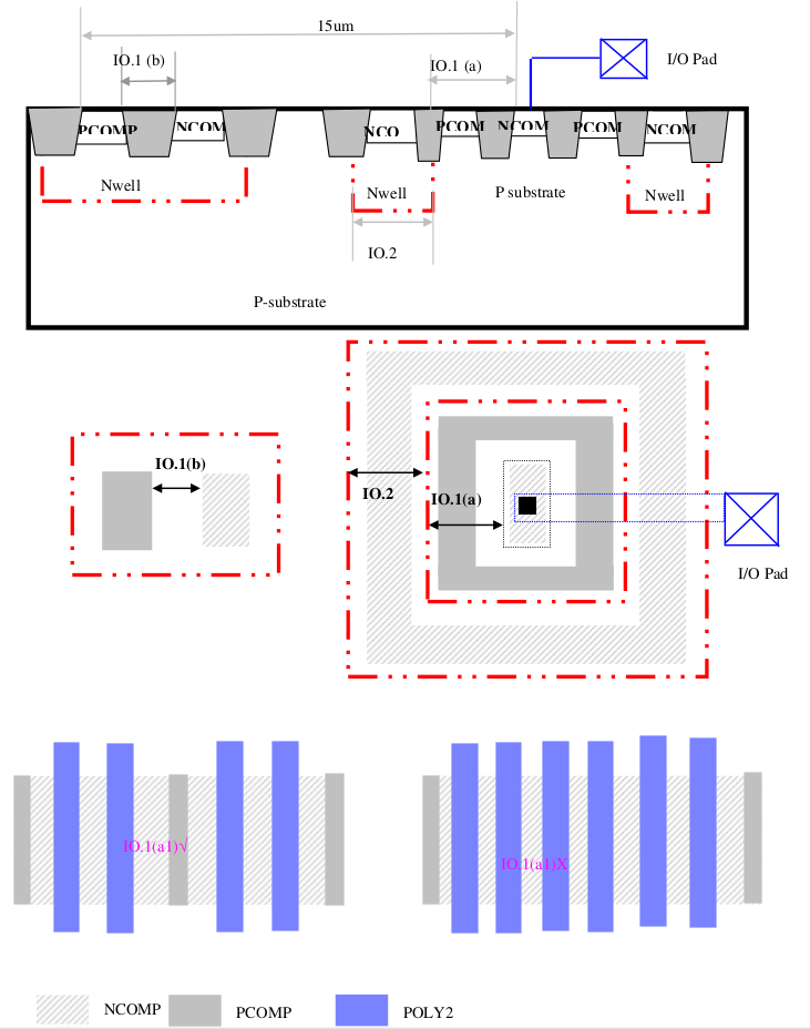
IO.1 |
(a1) NCOMP in PSub directly connected to I/O pad must be surrounded by Psub tap inside the Psub without any PCOMP in NWELL in between (Exclude the case when each NMOS transistor have full width butting to well tap). |
|||
(a2) It should also be directly surrounded by an Nwell guard ring (Non broken NCOMP ring inside Nwelll). Nwell guard ring shall be connected to the most positive supply. Max space of Nwell guard ring to the NCOMP in Psub directly connected to I/O pad. |
15 |
15 |
Rule |
|
pad (marked by Latchup_MK): Max Nwell tap distance to PCOMP inside Nwell (irrespective of its direct connection to Pad) |
2 |
2 |
Rule |
|
IO.2 |
Minimum recommended Nwell guard ring width: (Maximize contact to guard uniformly. As a guideline, ratio of total contact area to the active area of the guard ring should be more than 5%). |
2 |
2 |
Rule |
RULE NO. |
DESCRIPTION |
LV |
MV |
Comment |
FOR LV and MV |
||||
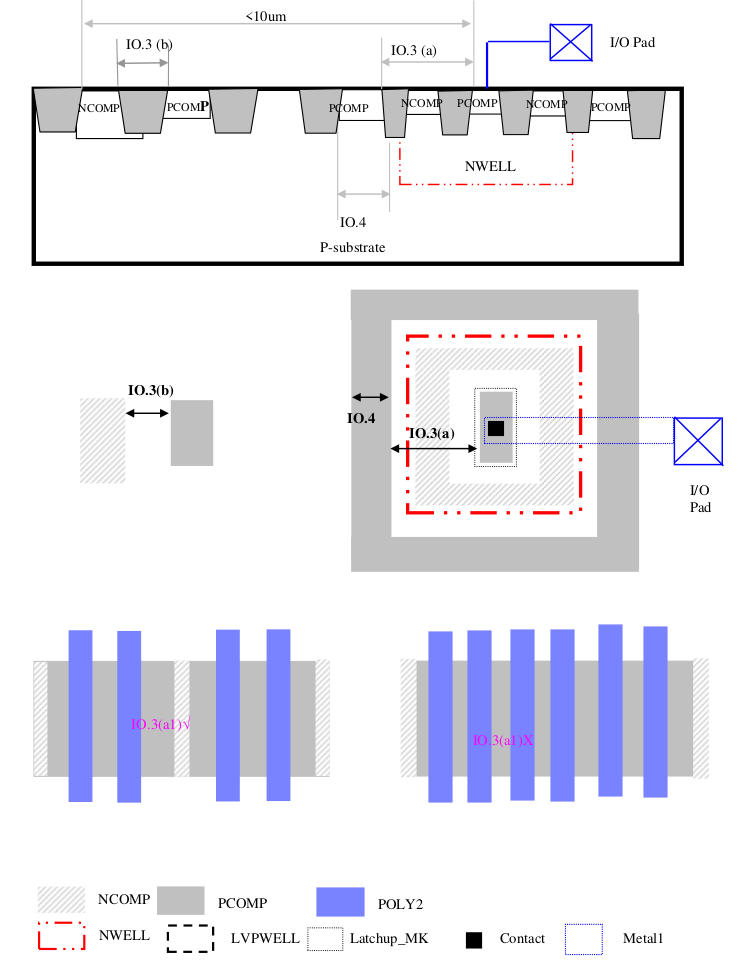
IO.3 |
a1) PCOMP in Nwell directly connected to I/O pad must be surrounded by Nwell tap inside the Nwell (Exclude the case when each PMOS transistor have full width butting to well tap). |
|||
a2) It should also be directly surrounded by PCOMP guard ring outside Nwell. PCOMP guard ring shall be connected to the lowest potential. Max space of guard ring PCOMP to the PCOMP in Nwell directly connected to the I/O pad. |
15 |
15 |
Rule |
|
b) Within 10um from the edge of the PCOMP connected to I/O Pad (marked by Latchup_MK): Max P substrate tap distance to NCOMP outside Nwell (irrespective of its direct connection to Pad) |
5 |
5 |
Rule |
|
IO.4 |
Minimum recommended PCOMP guard ring width: (Maximize contact to guard uniformly. As a guideline, ratio of total contact area to the active area of the guard ring should be more than 5%). |
2 |
2 |
Rule |