11.1 5V SRAM
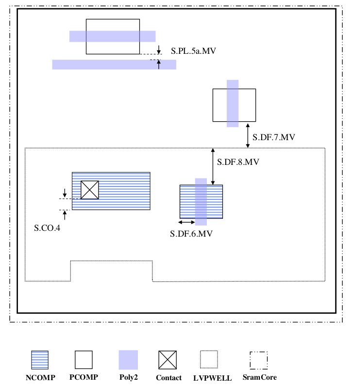
SramCore layer is used to mark SRAM cells. 5V SRAM cells with marking layer V5_XTOR should follow below specific rules which is different from 3.3V/(5V)6V rules.
RULE NO. |
DESCRIPTION |
LAYOUT RULE (5V) |
S.DF.4c_MV |
Min. (Nwell overlap of PCOMP) outside DNWELL |
0.45 |
S.DF.6_MV |
Min. COMP extend beyond gate (it also means source/drain overhang) |
0.32 |
S.DF.7_MV |
Min. (LVPWELL Spacer to PCOMP) inside DNWELL |
0.45 |
S.DF.8_MV |
Min. (LVPWELL overlap of NCOMP) Inside DNWELL |
0.45 |
S.DF.16_MV |
Min. space from (Nwell outside DNWELL) to (NCOMP outside Nwell and DNWELL). |
0.45 |
S.PL.5a_MV |
Space from field Poly2 to unrelated COMP Spacer from field Poly2 to Guard-ring |
0.12 |
S.PL.5b_MV |
Space from field Poly2 to related COMP |
0.12 |
S.CO.4_MV |
COMP overlap of contact |
0.04 |
Below Cell Description provides information about SRAM cell (1) and transistors.
Cell name |
13P5 |
Cell horizontal ( X ) dimension |
3 |
Cell vertical ( Y ) dimension |
4.5 |
Cell area (mm2) |
13.5 |
Grid |
0.005 |
Cell pull-up PMOS transistor (W/L) (2) |
0.6/0.6 |
Cell pull-down NMOS transistor (W/L) (2) |
0.95/0.6 |
Cell pass-gate NMOS transistor (W/L) (2) |
0.6/0.77 |
Beta ratio (pull-down W/L over pass-gate W/L) |
2.03 |
SRMA devices are allowed to be inside or outside of DNWELL.
SRAM devices follow the logic 5V/6V SPICE models.