gf180mcu_fd_ip_sram__sram64x8m8wm1
gf180mcu_fd_ip_sram__sram64x8m8wm1
180nm 5V Green synchronous single port SRAM
Memory Macro IP
Datasheet
Features
Uses 180nm 5V Green CMOS 13.5um2 6 transistors bitcell
64 words X 8 bits, mux 8 Instance
Periphery circuitry uses 5V transistors
Operating voltage is 1.62V to 5.50V
Operating temperature is -40 degC to 125 degC
Minimum 3 layers of metals required: Metal1, Metal2, Metal3
Bit write mask
Self timed operation to reduce power
Separate data in and data out ports
Macro cell name: gf180mcu_fd_ip_sram__sram64x8m8wm1
1.0 Pins Description
Signal |
Direction |
Description |
CLK |
Input |
Clock for the memory. Rising edge triggers operation. All inputs are latched at rising edge of the clock signal |
CEN |
Input |
Memory Enable, Active Low. When CEN is Low, the memory is enabled. When CEN input is High, the memory is deactivated but internal states are retained. CEN must be high before 1st running cycle. |
A[6:0] |
Input |
Address Input. This Address input port is used to address the location to be written during the write cycle and read during the read cycle. |
GWEN |
Input |
Write Enable Input. The RAM is in write cycle when GWEN is low. The RAM is in read cycle when GWEN is high. |
WEN[7:0] |
Input |
Bit Write Mask, Active Low. When the memory is in the write cycle, selectively write into individual outputs are controlled by WEN[7:0]. For example, if CEN, GWEN, WEN[0] are low and WEN[7:1] are high, only D[0] will write into the addressed location and D[7:1] will be ignored during CLK low to high transition. |
D[7:0] |
Input |
Data input bus. The data input bus is used to write data into the memory location specified by address input port during the write cycle. |
Q[7:0] |
output |
Data output bus. It outputs the contents of the memory location addressed by the Address Input signals. |
VDD |
Power |
Power pin. |
VSS |
Ground |
Ground pin. |
2.0 Truth Table
CLK |
CEN |
GWEN |
WEN |
A |
D |
Q |
status |
H |
X |
X |
X |
X |
Hold previous data |
Standby mode |
|
L |
H |
X |
A |
X |
Q |
Read mode |
|
L |
L |
H |
A |
D |
Hold previous data |
Write mode |
|
L |
L |
L |
A |
D |
Hold previous data |
Mask mode |
|
other |
X |
X |
X |
X |
X |
Hold previous data |
Unchanged |
Note
X: don’t care
3.0 Capacitance loading ( fF ) @ TT, 25°c
Voltage |
CLK |
CEN |
GWEN |
WEN |
A |
D |
5.0v |
296.201 |
17.6988 |
49.6735 |
7.84667 |
34.5188 |
16.5528 |
3.3v |
291.776 |
17.7783 |
48.1872 |
7.64901 |
34.5983 |
16.4468 |
1.8v |
280.919 |
17.7614 |
44.4991 |
7.15847 |
34.5814 |
16.1834 |
4.0 Power Consumption ( uW )
Condition of AC Write power is all data input pins switch and AC Read power is all address input and data output pins switch at 1MHz
4.1 5.0V Power
Condition |
DC standby |
AC Write |
AC Read |
TT corner, 5.00v, 25°c |
0.00013 |
859.2 |
770.85 |
SS corner, 4.50v, -40°c |
0.00011 |
670.77 |
603.675 |
SS corner, 4.50v, 125°c |
0.00014 |
701.798 |
630.697 |
FF corner, 5.50v, 125°c |
0.00946 |
1103.25 |
991.21 |
FF corner, 5.50v, -40°c |
0.00016 |
1046.15 |
940.445 |
4.2 3.3V Power
Condition |
DC standby |
AC Write |
AC Read |
TT corner, 3.3v, 25°c |
0.00006 |
342.144 |
310.2 |
SS corner, 3.0v, -40°c |
0.00005 |
273.045 |
249.09 |
SS corner, 3.6v, 125°c |
0.00006 |
289.68 |
263.76 |
FF corner, 3.6v, 125°c |
0.0037 |
441.252 |
395.91 |
FF corner, 3.6v, -40°c |
0.00007 |
409.23 |
368.748 |
4.3 1.8V Power
Condition |
DC standby |
AC Write |
AC Read |
TT corner, 1.8v, 25°c |
0.00002 |
92.043 |
84.3399 |
SS corner, 1.62v, -40°c |
0.00001 |
72.2552 |
67.2535 |
SS corner, 1.62v, 125°c |
0.00002 |
77.4279 |
71.1626 |
FF corner, 1.98v, 125°c |
0.0012 |
120.582 |
108.841 |
FF corner,1.98v, -40°c |
0.00002 |
110.484 |
100.495 |
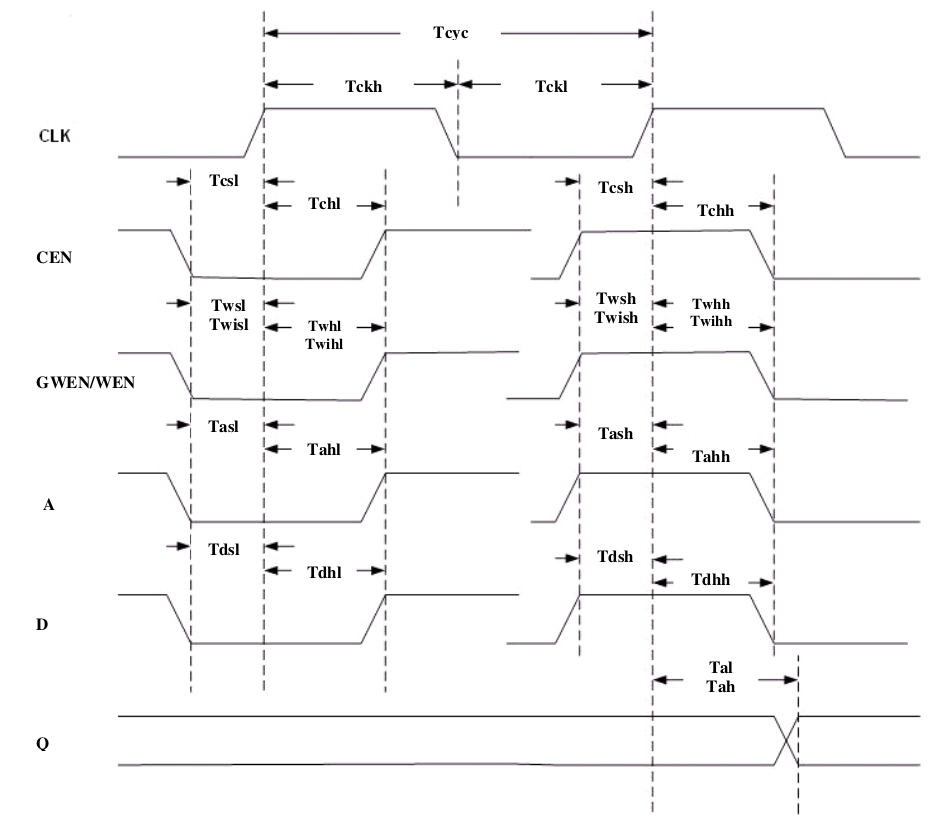
5.0 AC Characteristics
The timing and power values measured from the input slew of 20ps on clock pin, 20ps on signal and output load .01pF.
5.1 5.0V AC Characteristics
Symbol |
Parameter Description |
SNSP Process 4.5v, -40C |
SNSP Process 4.5v, 125C |
Typical Process 5.0v, 25C |
FNFP Process 5.5v, 125C |
FNFP Process 5.5v, -40C |
unit |
Tcyc |
Min clock period |
7.1094 |
10.2796 |
5.7473 |
5.3301 |
3.7332 |
ns |
Tckh |
Min clock high time |
3.2696 |
3.9625 |
2.2315 |
2.3664 |
1.4138 |
ns |
Tckl |
Min clock low time |
2.723 |
4.8463 |
2.5397 |
2.4258 |
1.355 |
ns |
Tcsl |
CEN set up time ( CEN = L ) |
0.4573 |
0.5866 |
0.4058 |
0.3883 |
0.3234 |
ns |
Tchl |
CEN hold time ( CEN = L ) |
1.2309 |
1.8505 |
1.1082 |
1.0785 |
0.764 |
ns |
Tcsh |
CEN set up time ( CEN = H ) |
0.514 |
0.6623 |
0.4352 |
0.4114 |
0.3381 |
ns |
Tchh |
CEN hold time ( CEN = H ) |
1.2875 |
1.9179 |
1.1376 |
1.1016 |
0.7788 |
ns |
Twsl |
GWEN set up time ( GWEN = L ) |
0.719 |
1.015 |
0.63 |
0.5885 |
0.4551 |
ns |
Twhl |
GWEN hold time ( GWEN = L ) |
0.9841 |
1.3576 |
0.8289 |
0.7912 |
0.5933 |
ns |
Twsh |
GWEN set up time ( GWEN = H ) |
0.6762 |
0.9362 |
0.592 |
0.563 |
0.4351 |
ns |
Twhh |
GWEN hold time ( GWEN = H ) |
0.5182 |
0.6761 |
0.456 |
0.4575 |
0.3629 |
ns |
Twisl |
WEN set up time ( WEN = L ) |
0.2931 |
0.3655 |
0.2719 |
0.244 |
0.2246 |
ns |
Twihl |
WEN hold time ( WEN = L ) |
0.9867 |
1.3576 |
0.8289 |
0.7912 |
0.5933 |
ns |
Twish |
WEN set up time ( WEN = H ) |
0 |
0 |
0 |
0 |
0 |
ns |
Twihh |
WEN hold time ( WEN = H ) |
0.5225 |
0.6786 |
0.4561 |
0.4575 |
0.3629 |
ns |
Tasl |
A set up time ( A = L ) |
0.8445 |
1.095 |
0.7027 |
0.6325 |
0.5165 |
ns |
Tahl |
A hold time ( A = L ) |
0.6188 |
0.7925 |
0.5272 |
0.492 |
0.4005 |
ns |
Tash |
A set up time ( A = H ) |
0.6391 |
0.8833 |
0.537 |
0.4936 |
0.3872 |
ns |
Tahh |
A hold time ( A = H ) |
0.6421 |
0.8303 |
0.5416 |
0.5018 |
0.406 |
ns |
Tdsl |
D set up time ( D = L ) |
0.1233 |
0.1049 |
0.1234 |
0.1046 |
0.1296 |
ns |
Tdhl |
D hold time ( D = L ) |
0.5086 |
0.6605 |
0.4518 |
0.4675 |
0.3608 |
ns |
Tdsh |
D set up time ( D = H ) |
0.6006 |
0.7833 |
0.4892 |
0.4136 |
0.3622 |
ns |
Tdhh |
D hold time ( D= H ) |
0.7431 |
1.0139 |
0.6432 |
0.6316 |
0.4818 |
ns |
Tah |
Clock high to Q high |
5.2963 |
7.7968 |
4.339 |
4.0561 |
2.7985 |
ns |
Tal |
Clock high to Q low |
5.4809 |
8.0592 |
4.4822 |
4.1672 |
2.8862 |
ns |
5.2 3.3V AC Characteristics
Symbol
Parameter
description
SNSP
Process
3.0v, -40C
SNSP
Process
3.0, 125C
Typical
Process
3.3v, 25C
FNFP
Process
3.6v, 125C
FNFP
Process
3.6v, -40C
unit
Tcyc
Min clock period
11.0881
16.3302
8.2602
7.1405
4.8003
ns
Tckh
Min clock high time
5.2766
4.546
2.6935
3.4945
2.3063
ns
Tckl
Min clock low time
4.0239
7.031
3.0279
3.1873
2.0473
ns
Tcsl
CEN set up time
( CEN = L )
0.6574
0.8496
0.5408
0.497
0.4055
ns
Tchl
CEN hold time
( CEN = L )
1.8972
2.8488
1.5921
1.4759
1.0202
ns
Tcsh
CEN set up time
( CEN = H )
0.8078
1.078
0.6156
0.5383
0.4256
ns
Tchh
CEN hold time
( CEN = H )
2.0022
2.9741
1.6413
1.5021
1.0371
ns
Twsl
GWEN set up time
( GWEN = L )
1.1603
1.6477
0.9192
0.8133
0.601
ns
Twhl
GWEN hold time
( GWEN = L )
1.426
2.0375
1.1276
1.0157
0.7499
ns
Twsh
GWEN set up time
( GWEN = H )
1.0297
1.4308
0.8248
0.742
0.5575
ns
Twhh
GWEN hold time
( GWEN = H )
0.6921
0.962
0.5782
0.5566
0.4374
ns
Twisl
WEN set up time
( WEN = L )
0.4664
0.5547
0.3886
0.337
0.2926
ns
Twihl
WEN hold time
( WEN = L )
1.4269
2.0375
1.1276
1.016
0.7505
ns
Twish
WEN set up time
( WEN = H )
0
0
0
0
0
ns
Twihh
WEN hold time
( WEN = H )
0.6944
0.962
0.5789
0.5566
0.4374
ns
Tasl
A set up time
( A = L )
1.2506
1.5795
0.9573
0.8183
0.6528
ns
Tahl
A hold time
( A = L )
0.8435
1.1028
0.6808
0.6072
0.4906
ns
Tash
A set up time
( A = H )
1.0439
1.3746
0.7931
0.6787
0.5232
ns
Tahh
A hold time
( A = H )
0.9133
1.1999
0.7195
0.6323
0.5058
ns
Tdsl
D set up time
( D = L )
0.182
0.1272
0.1649
0.1445
0.1652
ns
Tdhl
D hold time
( D = L )
0.5964
0.8295
0.5427
0.5413
0.421
ns
Tdsh
D set up time
( D = H )
1.0245
1.2872
0.7225
0.5774
0.4764
ns
Tdhh
D hold time
( D= H )
1.0708
1.5056
0.8569
0.7908
0.5979
ns
Tah
Clock high to Q
high
8.1919
11.9542
6.1696
5.4029
3.6754
ns
Tal
Clock high to Q low
8.5514
12.456
6.417
5.5901
3.8098
ns
5.3 1.8V AC Characteristics
Symbol |
Parameter description |
SNSP Process 1.62v, -40C |
SNSP Process 1.62v, 125C |
Typical Process 1.8v, 25C |
FNFP Process 1.98v, 125C |
FNFP Process 1.98v, -40C |
unit |
Tcyc |
Min clock period |
46.9428 |
50.9738 |
21.4387 |
13.8797 |
10.1117 |
ns |
Tckh |
Min clock high time |
17.8048 |
12.4148 |
5.5918 |
3.916 |
4.9481 |
ns |
Tckl |
Min clock low time |
20.3458 |
23.4901 |
9.3467 |
5.9066 |
4.7369 |
ns |
Tcsl |
CEN set up time ( CEN = L ) |
2.3723 |
2.4627 |
1.1531 |
0.8039 |
0.6538 |
ns |
Tchl |
CEN hold time ( CEN = L ) |
7.2625 |
8.1371 |
3.8299 |
2.7467 |
2.0012 |
ns |
Tcsh |
CEN set up time ( CEN = H ) |
3.5906 |
3.6093 |
1.5645 |
0.973 |
0.7991 |
ns |
Tchh |
CEN hold time ( CEN = H ) |
8.1157 |
8.8493 |
4.0493 |
2.806 |
2.0585 |
ns |
Twsl |
GWEN set up time ( GWEN = L ) |
5.437 |
5.6091 |
2.4169 |
1.5313 |
1.1881 |
ns |
Twhl |
GWEN hold time ( GWEN = L ) |
6.4375 |
6.9235 |
2.5611 |
1.7504 |
1.3035 |
ns |
Twsh |
GWEN set up time ( GWEN = H ) |
3.7804 |
4.1608 |
1.8848 |
1.2969 |
1.004 |
ns |
Twhh |
GWEN hold time ( GWEN = H ) |
3.7001 |
3.9258 |
1.2605 |
0.8555 |
0.6691 |
ns |
Twisl |
WEN set up time ( WEN = L ) |
0.089 |
0.1242 |
0.7187 |
0.566 |
0.5008 |
ns |
Twihl |
WEN hold time ( WEN = L ) |
6.47 |
6.9448 |
2.572 |
1.7504 |
1.3079 |
ns |
Twish |
WEN set up time ( WEN = H ) |
0 |
0 |
0 |
0 |
0 |
ns |
Twihh |
WEN hold time ( WEN = H ) |
3.7346 |
3.9386 |
1.2609 |
0.8555 |
0.6691 |
ns |
Tasl |
A set up time ( A = L ) |
2.7499 |
2.7972 |
1.9241 |
1.362 |
1.1243 |
ns |
Tahl |
A hold time ( A = L ) |
2.3664 |
2.566 |
1.276 |
0.938 |
0.7583 |
ns |
Tash |
A set up time ( A = H ) |
3.4976 |
3.5401 |
1.811 |
1.2267 |
1.0163 |
ns |
Tahh |
A hold time ( A = H ) |
2.9875 |
3.1533 |
1.4855 |
1.0268 |
0.8386 |
ns |
Tdsl |
D set up time ( D = L ) |
0 |
0 |
0.0245 |
0.1435 |
0.1899 |
ns |
Tdhl |
D hold time ( D = L ) |
2.9813 |
3.0888 |
0.9452 |
0.7355 |
0.5491 |
ns |
Tdsh |
D set up time ( D = H ) |
3.4777 |
3.3172 |
1.841 |
1.061 |
0.9368 |
ns |
Tdhh |
D hold time ( D= H ) |
5.6811 |
5.9063 |
2.0886 |
1.3397 |
1.0391 |
ns |
Tah |
Clock high to Q high |
32.2344 |
35.5512 |
15.2892 |
10.1268 |
7.4477 |
ns |
Tal |
Clock high to Q low |
34.7448 |
37.83 |
16.1808 |
10.5967 |
7.8205 |
ns |
AC Timing Waveform Chart
6.0 Physical Dimensions
Width(um) |
Height(um) |
Area(um^2) |
431.86 |
232.88 |
100571.5568 |